Identification of Equivalent Logic Gate Circuit
If and are the inputs, the given circuit works as __________.
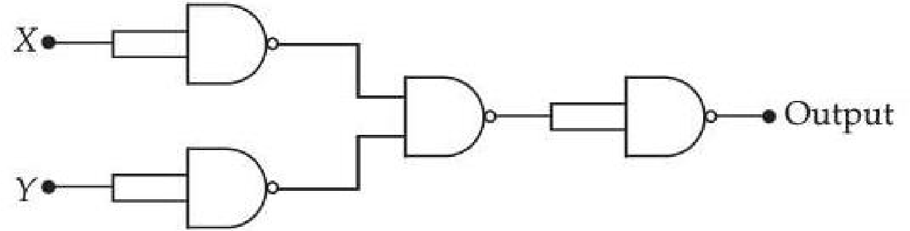
Options
OR gate
AND gate
NAND gate
NOR gate
Topics & Concepts
Step-by-Step Solution
To determine the logic gate equivalent of the given circuit, let us analyze the operation of each gate step-by-step.
From the circuit diagram, all four gates are two-input NAND gates.
Step 1: First Stage Gates (Inverters)
-
Top-Left NAND Gate: Both inputs are connected together to signal . The output of this gate is given by:
-
Bottom-Left NAND Gate: Both inputs are connected together to signal . The output of this gate is given by:
Step 2: Second Stage Gate
The middle NAND gate takes and as its inputs. The output of this gate is:
Using De Morgan's Theorem ():
Step 3: Final Stage Gate
The output is fed into both inputs of the final NAND gate. The final output of the circuit is:
Substituting :
Conclusion:
The Boolean expression for the output is , which represents the operation of a NOR gate.
Correct Answer: NOR gate (Option D)